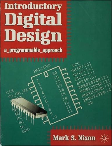
By Mark S. Nixon (auth.)
Read Online or Download Introductory Digital Design: a_programmable_approach PDF
Best electronics books

Dielectric Materials and Devices
This specific stand on my own quantity information new advancements in dielectric ceramics. It presents complete experiences of latest fabrics and product options and comprises subject matters similar to fabrics synthesis and processing, relaxors & novel compositions, dielectric loss mechanisms, multiplayer ceramic units, and price research of tomorrow’s electrical units.

Analog/RF and Mixed-Signal Circuit Systematic Design
Although within the electronic area, designers can take complete advantages of IPs and layout automation instruments to synthesize and layout very complicated structures, the analog designers’ job continues to be regarded as a ‘handcraft’, bulky and extremely time eating technique. hence, great efforts are being deployed to strengthen new layout methodologies within the analog/RF and mixed-signal domain names.
One of many most powerful tendencies within the layout and manufacture of recent electronics applications and assemblies is the usage of floor mount expertise as a substitute for through-hole tech nology. The mounting of digital units and parts onto the skin of a published wiring board or different substrate deals many benefits over putting the leads of units or elements into holes.
- Electrical and Electronic Principles and Technology (3rd Edition)
- Electrical Characterization of Organic Electronic Materials and Devices
- Teach Yourself Electricity and Electronics (4th Edition)
- Biopolymer Composites in Electronics
- Tom Swift and the Electronic Hydrolung (Book 18 in the Tom Swift Jr series)
Additional resources for Introductory Digital Design: a_programmable_approach
Sample text
This is a guarantee that if an input is within the range specified for the input levels then the output of the circuit is guaranteed to be within a range specified for the output voltage levels. If you buy a circuit which does not conform to this specification you can return it to the manufacturer for replacement. If an input voltage level falls outside the range specified for a valid logic level then it naturally becomes invalid and the circuit will not respond correctly. This might occur because noise has corrupted the transmission line connecting two logic gates.
Since both NAND and NOR gates can be used to implement OR and AND, respectively, by inverting the inputs any function can be implemented using NAND or NOR gates only. 11. Combinational Logic Design 31 De Morgan's law is true semantically, too. Compare 'I cannot water the garden with a leaky bucket and no water' with '/ can only water the garden with a good bucket and water'. You can therefore use de Morgan's law to simplify complicated IF statements when programming. Two other laws can be derived from this algebra: A+A·B=A A+A·B=A+B For proof, for the first of these A+ A · B =A · (1 +B)= A · 1 =A for the second, by substitution for A + A · B = A, then A+ A · B =A+ A · B + A · B =A+ B(A + A)= A+ B · 1 =A+ B These give reduced circuits: A+A·B A--------A A+AB In other words, why use gates when they are redundant?
Since they only approximate their perfect version they have resistance. Their resistance implies that the voltage across them increases with an increase in the current through them. When the voltage drop increases the output voltage falls, eventually to beneath that guaranteed as a valid output. The increase in current will be due to increasing the number of gates connected to the output. If we connect more gates than the specified maximum (the fan-out of the device), the output voltage level will not be valid as specified for the device.