
By Lee W. Ritchey
Name correct the 1st Time: a pragmatic guide on excessive pace PCB and process layout, quantity 1 correct the 1st Time: a realistic instruction manual on excessive velocity PCB and procedure layout, Kella J. Knack writer Lee W. Ritchey Editor Kella J. Knack version illustrated writer rushing side, 2003 ISBN 0974193607, 9780974193601 size 288 pages
Read Online or Download Right the First Time: a Practical Handbook on High Speed Pcb and System Design PDF
Similar electronics books

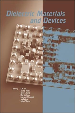
Dielectric Materials and Devices
This special stand by myself quantity info new advancements in dielectric ceramics. It offers accomplished reports of recent fabrics and product techniques and contains issues comparable to fabrics synthesis and processing, relaxors & novel compositions, dielectric loss mechanisms, multiplayer ceramic units, and value research of tomorrow’s electrical units.

Analog/RF and Mixed-Signal Circuit Systematic Design
Even though within the electronic area, designers can take complete advantages of IPs and layout automation instruments to synthesize and layout very advanced structures, the analog designers’ activity continues to be regarded as a ‘handcraft’, bulky and intensely time eating technique. therefore, super efforts are being deployed to enhance new layout methodologies within the analog/RF and mixed-signal domain names.
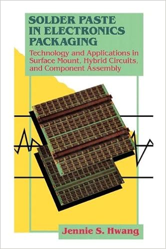
One of many most powerful traits within the layout and manufacture of recent electronics programs and assemblies is the usage of floor mount expertise as an alternative for through-hole tech nology. The mounting of digital units and elements onto the skin of a broadcast wiring board or different substrate deals many benefits over putting the leads of units or elements into holes.
- Electronic Materials
- Ten Essential Skills for Electrical Engineers
- Common Ground in Electronically Mediated Communication (Synthesis Lectures on Information Concepts, Retrieval, and Services)
- Electrical And Electronic Principles And Technology
- Basic Principles of Electronics. Thermionics
Additional info for Right the First Time: a Practical Handbook on High Speed Pcb and System Design
Example text
The first approach can only be used on surface layers of microwave/RF PCBs, while the second approach is used on logic PCBs. Circuit element sizes- All components mounted in packages have their performance degraded due to unwanted package parasitics, such as lead inductance, lead capacitance and lead-to-lead crosstalk. The faster a component must operate, the more these unwanted parasitics degrade performance. Minimizing the size of the package in which the component is mounted minimizes these parasitics.
The publishers of applications notes should do the same. Actually, publishers of application notes and guidelines should be held to an even higher standard. This is especially true since users of these application notes and guidelines expect the design rules contained within them to be valid and often bet not only their designs but also their entire companies on them. The unfortunate truth is that most applications notes are not prepared with this level of rigor. Even worse, some engineers who give out rules of thumb and are asked to support their rules with scientific analysis or experiment are offended that the questioner doesn’t trust them.
The same part of the tolerance budget used for impedance mismatch will be used to compensate for dielectric losses. Skin effect losses are associated with current flowing in conductors crowding into a thin layer near the surface at high frequencies. This loss gets larger as frequencies increase. It is compensated for by plating the outer surfaces of conductors with gold to increase conductivity or by increasing the width of traces to create more surface area. The first approach can only be used on surface layers of microwave/RF PCBs, while the second approach is used on logic PCBs.